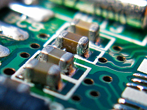
Example 3: Implementation of a ceramic
thin-film capacitor deposition production
process for a large semiconductor company.
OBJECTIVES: Due to our experience in the field of sol-gel technology and its application to the formation of ceramic thin-films, we were hired by a large, ISO 9001 registered, publicly-traded semiconductor company to develop a manufacturable version of a spin-coating method for creating high-dielectric ceramic thin-films of Barium Strontium Titanate (BST) for use in the manufacture of miniaturized capacitor arrays.
EXECUTION: Extensive modifications of the basic chemical preparation process were required to make it production capable. The pilot-plant scale facility that we put in place generated product with batch-to-batch repeatability greater than that obtainable by related products on the market. The synthesis process was transferred to manufacturing complete with ISO compliant documentation. Additional work on this project involved implementation of automated equipment for substrate coating and thermal processing. In addition, due to our understanding of thin-film materials science, we were also extensively involved in several other aspects of this project, such as thin-film sputter deposition and furnace process qualification. We employed extensive materials characterization and failure analysis methods to improve product quality and yield. Much of this failure analysis work involved collaboration with scientists at external labs, both in the United States and in Canada.
RESULTS: The spin-on chemical that was produced by this process ultimately was used to manufacture a substantial quantity of final sold product. In addition, we worked with the Marketing and Sales Deparment of this semiconductor company for 6 months exploring the possibility of selling this spin-on chemical as a New Product Introduction.